Introduction
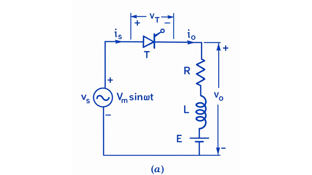
A single phase half wave controlled rectifier is a power electronic converter that converts single-phase AC voltage into a controlled DC output using a thyristor (SCR). By controlling the firing angle of the SCR, the average output voltage and current supplied to the load can be regulated.
When the load consists of Resistance (R), Inductance (L), and a DC back emf (E)—such as in DC motor armature circuits—the load is referred to as an RLE load. The presence of inductance and back emf significantly affects the conduction behavior, current continuity, and output characteristics of the rectifier.
Circuit Diagram
Working Operation
Positive Half Cycle (Conduction Interval)
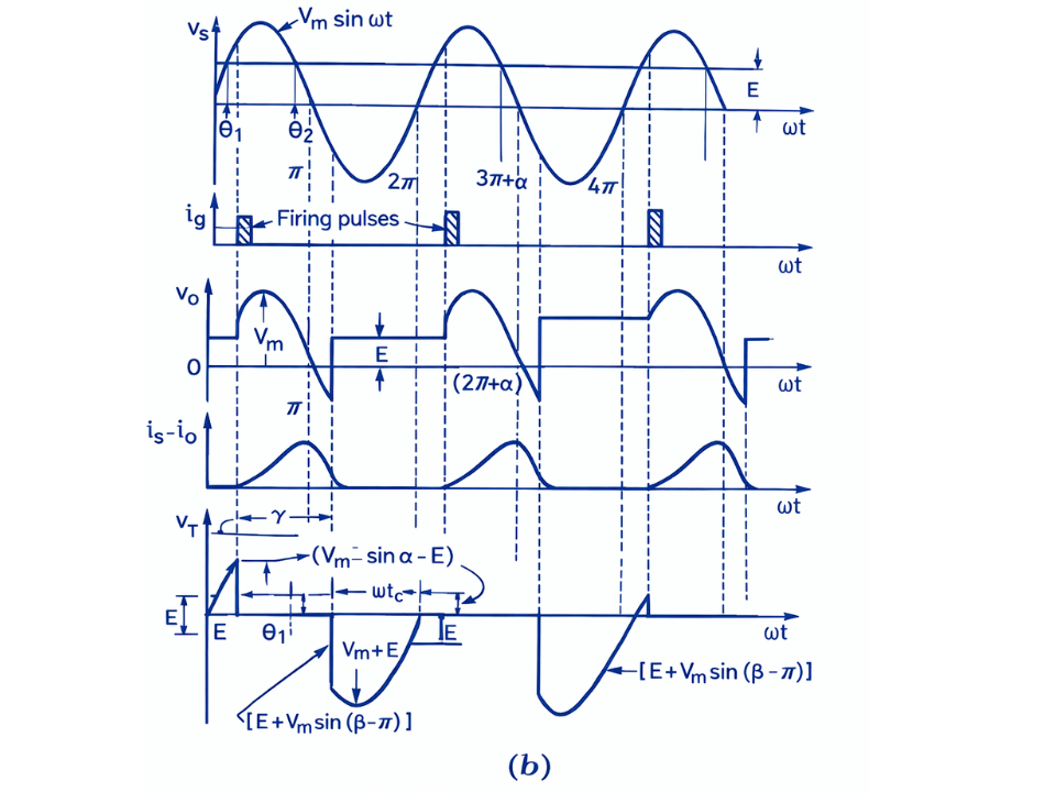
During the positive half cycle, the thyristor is fired at a firing angle such that . From to , the thyristor remains reverse biased and hence the load current , while the load voltage remains equal to the back emf, . At , the thyristor is triggered and turns ON. Immediately after triggering, the load voltage follows the source voltage and the load current begins to increase gradually due to the inductive nature of the load. As the conduction continues, the current rises and then decreases as the supply voltage reduces.
At , the instantaneous supply voltage becomes zero; however, due to the stored energy in the inductor, the load current does not fall to zero immediately. From to , the current continues to flow and during this interval the load voltage becomes negative and gradually decreases to zero. At , the load current finally reaches zero, and since the current becomes less than the holding current, the thyristor is naturally commutated and turns OFF automatically.
Due to the presence of inductance in the load, the current rises gradually and does not attain its peak value instantaneously. The back emf opposes the applied supply voltage, thereby reducing the effective voltage available across the load and limiting the rate of rise of current. During this conduction interval, the output voltage is equal to the instantaneous value of the supply voltage, and energy is transferred from the source to the load.
Negative Half Cycle (Blocking Interval)
During the negative half cycle, the thyristor is reverse biased and remains in the OFF state throughout this interval. From to , no load current flows, so , while the load voltage remains equal to the back emf, . Thus, no conduction takes place during the negative half cycle.
Output Waveform
Mathematical Expressions
Average Output Voltage
Hence, the average output voltage over one cycle is
Substituting ,
Applying limits to ,
Average Load Current
From the DC equivalent of the RLE load,
Hence,
Substituting ,
RMS Output Voltage
Using identity