
Introduction
A Single Phase Half Wave Controlled Rectifier with RL Load is a power electronic converter that converts single phase AC voltage into controlled DC using a thyristor (SCR) and a load consisting of resistance and inductance in series. The average output voltage is controlled by varying the firing angle of the SCR, while the inductance causes current continuity and delayed commutation.
Construction (Circuit Arrangement)
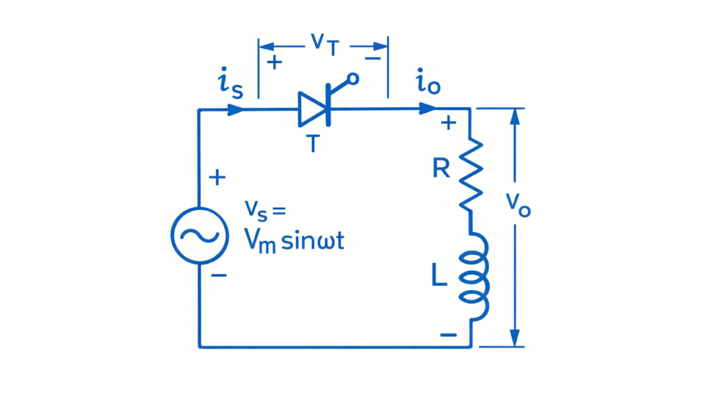
The circuit consists of:
- A single phase AC supply
- A thyristor (SCR) connected in series with the load
- A series combination of resistance and inductance as the load
- A gate triggering circuit to apply firing pulses at angle
The SCR is placed between the AC source and the RL load. The gate circuit controls the firing instant of the SCR. The resistive part limits the current, while the inductive part stores energy and maintains current continuity.
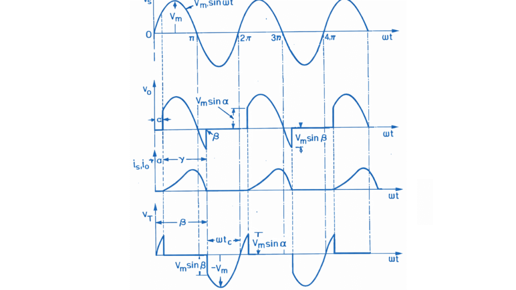
Working Principle
Positive Half Cycle
During the positive half cycle of the AC input, the thyristor (SCR) becomes forward biased since the anode is positive with respect to the cathode. However, conduction does not start immediately because the SCR remains in the forward blocking state until a gate triggering pulse is applied. From ωt = 0 up to the firing angle α, no current flows through the load and the output voltage remains zero. This interval is known as the delay period.
At the instant ωt = α, a gate pulse is applied and the SCR turns ON. Current begins to flow through the series RL load. Due to the presence of inductance, the current does not rise instantaneously but increases gradually and lags behind the voltage. The output voltage follows the input sinusoidal voltage and the inductor stores energy in the form of a magnetic field. The SCR continues to conduct throughout the remaining part of the positive half cycle up to ωt = π.
Negative Half Cycle
When the input voltage crosses zero at ωt = π and becomes negative, the SCR becomes reverse biased. Under normal conditions this would turn the SCR OFF, but in an RL load the current does not immediately fall to zero because of the energy stored in the inductor. The inductor maintains current flow in the same direction, and therefore the SCR continues to conduct even though the supply voltage has reversed polarity.
During this interval, the output voltage becomes negative while the load current remains positive. The stored energy in the inductor is gradually released and the current decreases slowly. Conduction continues until the current decays to zero at the extinction angle , where . At this point the current falls below the holding current and the SCR turns OFF naturally. This process is called natural commutation.
Output Waveform
Mathematical Expressions
Average (DC) Output Voltage
The average output voltage is calculated over the conduction interval
This expression shows that the average output voltage depends on both:
- Firing angle
- Extinction angle
Average (DC) Load Current
RMS Output Voltage
RMS Load Current
Rectification Efficiency
Rectification efficiency (η) is defined as the ratio of DC output power to the AC input power supplied to the rectifier.
DC Output Power
The average DC power delivered to the load is
From previous analysis:
Hence,
AC Input Power
The AC input power is the power dissipated in the load due to RMS current:
Efficiency Expression
Ripple Factor
Ripple factor indicates the amount of AC component present in the DC output. It is defined as: