What is Thyristor (SCR)?
A Silicon Controlled Rectifier (SCR) is a three-terminal, four-layer (PNPN), unidirectional power semiconductor device belonging to the thyristor family, which is used for controlled switching and regulation of high voltage and high current in power electronic circuits.
It operates as a bistable device that remains in the non-conducting (OFF) state under forward bias until a suitable gate triggering signal is applied, after which it switches to the conducting (ON) state and continues to conduct even after the removal of the gate signal until the anode current falls below the holding current.
The three terminals of an SCR are:
- Anode (A): Main current-carrying terminal connected to the positive supply
- Cathode (K): Main current-carrying terminal connected to the negative supply
- Gate (G): Control terminal used to initiate conduction
The four semiconductor layers form three junctions, designated as J1, J2, and J3, which determine the switching characteristics of the device.
Construction of SCR
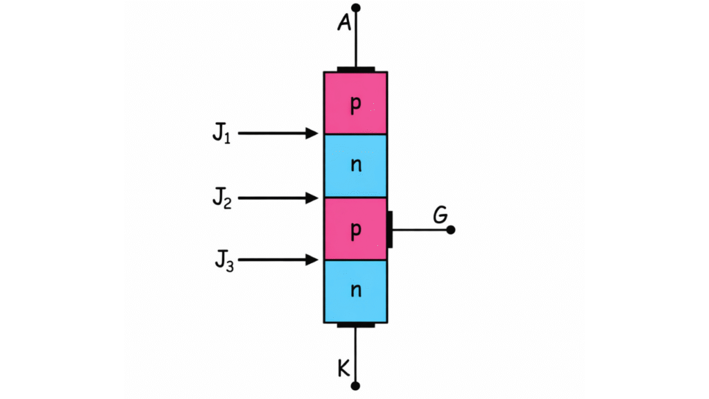
The SCR is fabricated using high-purity silicon and consists of four alternate layers arranged as P1–N1–P2–N2. The junctions formed between these layers are:
- J1: Between P1 and N1
- J2: Between N1 and P2
- J3: Between P2 and N2
The anode is connected to the outer P-layer (P1), the cathode is connected to the outer N-layer (N2), and the gate terminal is connected to the inner P-layer (P2).
The device structure results in a tightly coupled regenerative feedback mechanism between two internal transistors: a PNP transistor and an NPN transistor. This internal transistor model explains the latching and switching behavior of the SCR.
Modes of Operation of SCR
The operation of a Silicon Controlled Rectifier depends on the polarity of the applied voltage across the anode and cathode and on the gate signal. An SCR operates in three distinct modes, namely:
- Reverse Blocking Mode
- Forward Blocking Mode
- Forward Conduction Mode
Each mode corresponds to a particular biasing condition of the internal junctions J1, J2, and J3.
Reverse Blocking Mode
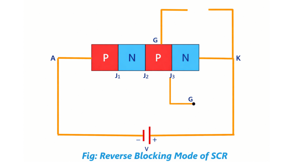
In this mode, the cathode is made positive with respect to the anode, and the gate terminal is kept open.
- Junctions J1 and J3 are reverse biased
- Junction J2 is forward biased
Since two of the three junctions are reverse biased, the SCR offers high reverse resistance and blocks the flow of current. Only a small reverse leakage current flows through the device.
If the reverse voltage exceeds the rated reverse breakdown voltage, avalanche breakdown may occur, leading to permanent damage. Hence, the SCR is normally operated below this limit in reverse blocking mode.
Forward Blocking Mode
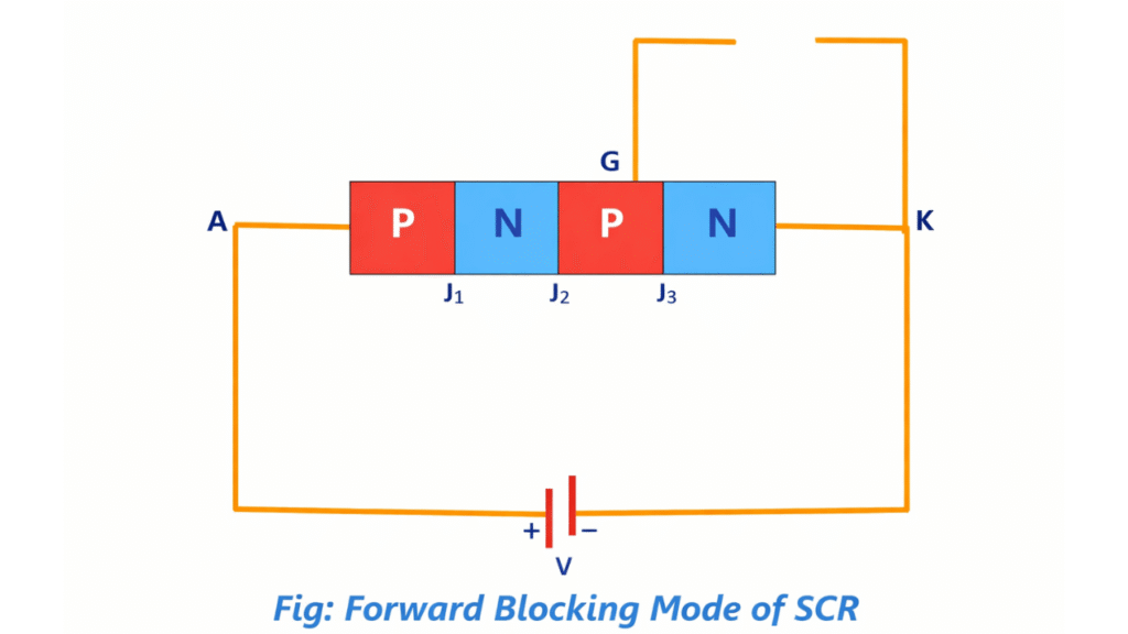
In this mode, the anode is made positive with respect to the cathode, but no gate signal is applied.
- Junctions J1 and J3 are forward biased
- Junction J2 is reverse biased
Due to the reverse-biased central junction J2, the SCR remains in the OFF state and blocks the forward current. Only a small forward leakage current flows. In this condition, the SCR behaves like a forward-biased diode with high resistance.
If the anode-to-cathode voltage is increased beyond a certain value called the forward breakover voltage (V_BO), junction J2 breaks down and the SCR turns ON even without gate triggering. However, this method is not preferred due to the possibility of excessive current and device damage.
Forward Conduction Mode
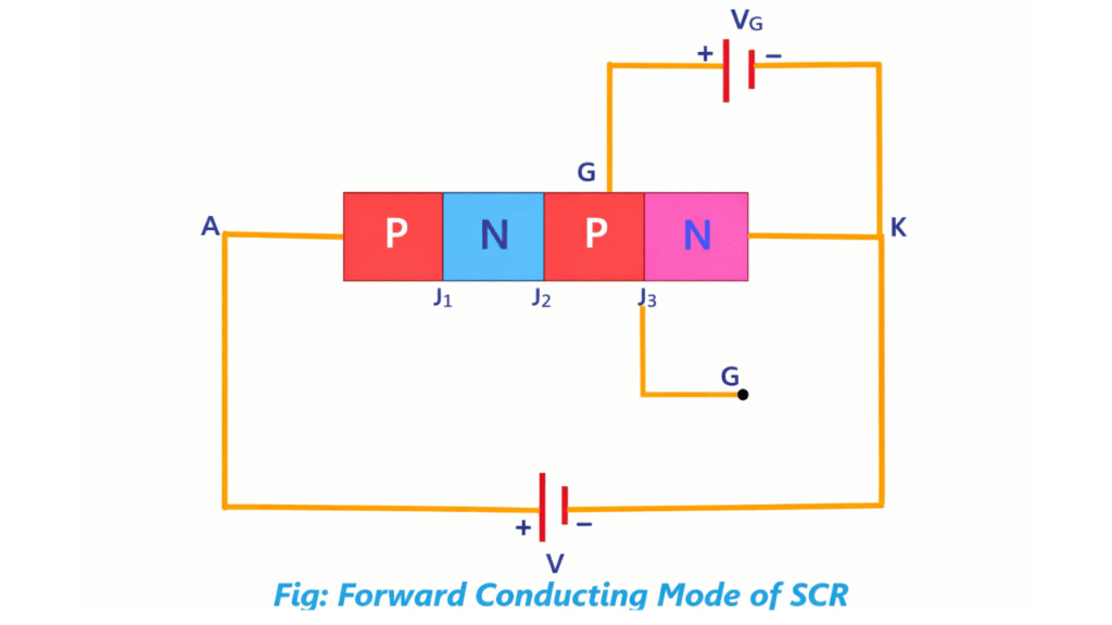
When the SCR is forward biased and a positive gate current is applied with respect to the cathode, the device enters the forward conduction mode.
- Carriers are injected into the inner P-layer through the gate
- The reverse bias at junction J2 is reduced
- Regenerative feedback between internal transistor pairs is initiated
As a result, all three junctions become forward biased, and the SCR switches to the ON state. The device now offers low forward resistance and conducts heavily from anode to cathode.
Once the SCR is turned ON, it remains ON even if the gate signal is removed. This phenomenon is known as latching. The SCR will turn OFF only when the anode current falls below a minimum value called the holding current.
V-I Characteristics of Silicon Controlled Rectifier (SCR):
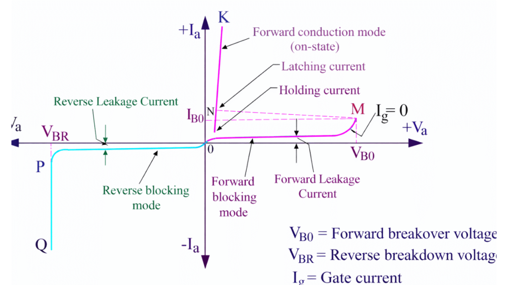
The V–I characteristics of a Silicon Controlled Rectifier describe the relationship between the anode current (Iₐ) and the anode-to-cathode voltage (Vₐ) under different operating conditions. The characteristic curve is divided into three main regions:
- Reverse Blocking Region
- Forward Blocking Region
- Forward Conduction Region
These regions explain the blocking, triggering, and conduction behavior of the SCR.
| Region | Biasing Condition | Junction Status | SCR State | Key Characteristics |
|---|---|---|---|---|
| Reverse Blocking Region | Cathode positive with respect to anode | J1, J3 reverse biased J2 forward biased |
OFF | Only reverse leakage current flows; breakdown at VBR |
| Forward Blocking Region | Anode positive, gate open | J1, J3 forward biased J2 reverse biased |
OFF | Forward leakage current flows; breakdown at VBO |
| Forward Conduction Region | Anode positive and gate triggered | All junctions forward biased | ON | Low forward voltage drop (≈ 1–2 V); heavy anode current flows |
Important Parameters in V–I Characteristics
Forward Breakover Voltage
It is the minimum anode-to-cathode forward voltage at which the SCR turns ON without gate triggering. Gate current reduces the value of V_BO.
Reverse Breakdown Voltage
It is the maximum reverse voltage that the SCR can withstand without entering breakdown. Beyond this voltage, the reverse current increases sharply.
Latching Current
It is the minimum anode current required to keep the SCR in the ON state immediately after triggering when the gate signal is removed. If the anode current is less than I_L, the SCR turns OFF.
Holding Current
It is the minimum anode current below which the SCR turns OFF during conduction. For proper operation, the anode current must always remain greater than the holding current.
Note:
Turn on methods of SCR
The turning on Process of the SCR is known as Triggering. In other words, turning the SCR from Forward-Blocking state to Forward-Conduction state is known as Triggering.
The various methods of SCR triggering are discussed here.
- Forward Voltage Triggering
- Thermal or Temperature Triggering
- Radiation or Light triggering
- dv/dt Triggering
- Gate Triggering
Two Transistor Analogy of SCR
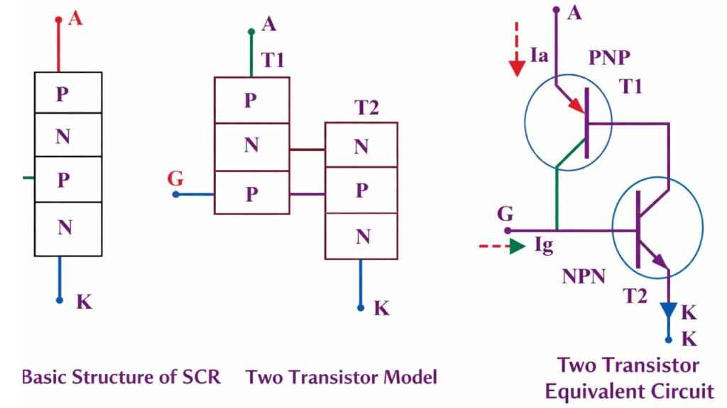
The PNPN structure of the SCR can be represented by two transistors:
- PNP transistor (T₁)
- NPN transistor (T₂)
The collector of each transistor is connected to the base of the other, forming a positive feedback loop. When a gate current is applied, conduction in one transistor increases the base current of the other, resulting in regenerative action. The SCR turns ON when:
This model explains the latching and switching behavior of the SCR.
Let,
- = Anode current
- = Collector current of PNP transistor (T₁)
- = Collector current of NPN transistor (T₂)
- = Gate current
- = Common-base current gain of T₁
- = Common-base current gain of T₂
From transistor theory:
where
= leakage currents of transistors
Since cathode current
The anode current is the sum of collector currents:
Substituting:
Expanding:
where
Rearranging the Equation
Final Expression for Anode Current
This is the fundamental SCR anode current equation derived from the two-transistor model.
| Advantages of SCR | Limitations of SCR |
|---|---|
| Capable of handling very high voltage and current | Unidirectional conduction only |
| Low forward voltage drop resulting in low conduction loss | Cannot be turned OFF by gate control |
| High efficiency in power conversion applications | Requires external commutation circuit for turn OFF in DC circuits |
| Simple and low-power gate triggering requirement | Slow switching speed compared to MOSFETs and IGBTs |
| Latching property simplifies control in many applications | Not suitable for high-frequency applications |
| High surge current capability and rugged construction | Sensitive to dv/dt and di/dt effects |
| High reliability and long operational life | Requires snubber and protection circuits |
| Economical for medium and high power ratings | Produces harmonics in AC power control circuits |
| Suitable for both AC and DC power control | Poor performance at low current levels |
| Widely available in large current and voltage ratings | Gate loses control once the device is latched ON |
Applications of Silicon Controlled Rectifier (SCR)
- Controlled rectifiers
- DC motor speed control
- AC voltage regulators
- Light dimmers
- Battery chargers
- Inverters
- Cycloconverters
- HVDC transmission
- Soft starters
- Industrial heating
- Welding machines
Conclusion
The Silicon Controlled Rectifier is a fundamental power semiconductor device widely used in controlled power conversion and industrial applications. Its ability to handle high voltage and current with simple gate control makes it highly suitable for power regulation, motor control, and energy conversion systems. Despite the availability of faster devices, SCR continues to dominate medium and high-power applications due to its reliability, efficiency, and rugged construction.
Short FAQ – Silicon Controlled Rectifier (SCR)
What is a Silicon Controlled Rectifier (SCR)?
An SCR is a three-terminal, four-layer PNPN power semiconductor device used as a controlled switch for regulating high voltage and high current.
How is an SCR turned ON?
An SCR is turned ON by applying a positive gate current while it is forward biased or by increasing the anode-to-cathode voltage beyond the breakover voltage.
Can an SCR be turned OFF by gate control?
No, an SCR cannot be turned OFF by gate control. It turns OFF only when the anode current falls below the holding current.
What is the difference between latching current and holding current?
Latching current is the minimum current required to keep the SCR ON immediately after triggering, while holding current is the minimum current below which the SCR turns OFF during conduction.